Command Palette
Search for a command to run...
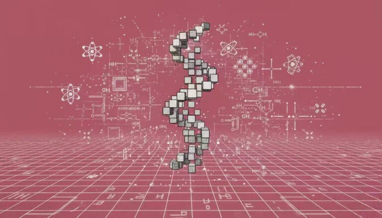
Based on Simulated Spectral Data of 2,000 Semiconductor Materials, the MIT Team Proposed DefectNet, Which Can Analyze Six Coexisting Substitution defects.
In biology, defects are generally considered harmful. However, in materials science, defects can be intentionally engineered to endow materials with new and useful properties. Today, atomic-level defects are carefully introduced into the manufacturing processes of products such as steel, semiconductors, and solar cells to improve strength, control conductivity, optimize performance, and more. For example, carrier concentration can be tuned through controlled doping in silicon; similarly, defect engineering in ultra-wide bandgap semiconductors can enhance their potential for use in next-generation power electronics.
While defect analysis has become a powerful tool, accurately measuring the different types and concentrations of defects in finished products remains extremely challenging, especially without cutting or damaging the final material. Engineers who are unaware of the defects present in the material may produce products with poor performance or unintended characteristics. Despite the abundance of existing defect characterization techniques, significant limitations remain in terms of sensitivity, selectivity, quantifiability, and destructiveness.
In this context,A research team from MIT has proposed a fundamental machine learning model called DefectNet, which can directly predict the chemical types and concentrations of substitution point defects from vibrational spectra measured in phonon density of states (PDoS).Even in the presence of multiple elements, this model is achievable. Trained on over 16,000 simulated spectral data points from 2,000 semiconductor materials, the model employs a customized attention mechanism to identify up to six different defect elements with concentrations ranging from 0.21 TP³T to 251 TP³T. The model demonstrates good generalization ability in unseen crystals containing 56 elements and can be fine-tuned using experimental data. Validation using inelastic scattering experimental data from SiGe alloys and MgB₂ superconductors demonstrates the model's accuracy and transferability.
The related research findings, titled "A foundation model for non-destructive defect identification from vibrational spectra," have been published as a preprint on arXiv.
Research highlights:
Combining vibrational spectroscopy measurements of phonon density of states (PDoS) with machine learning offers a promising pathway for non-destructive characterization and quantification of point defects in bulk materials.
* Introducing a spectral attention mechanism to address the issue that phonon spectra of defective and perfect crystals may be almost indistinguishable under low-concentration conditions.
* Introducing machine learning inter-atomic potentials (MLIPs) to address the challenge of high computational costs in phonon simulations based on density functional theory (DFT).
Paper address:
https://arxiv.org/abs/2506.00725
View more AI papers:
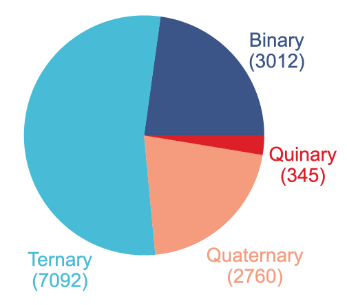
Dataset: A dataset built based on 2,000 perfect crystalline materials
The study constructed a dataset containing 16,000 doped supercells from 2,000 perfect crystalline materials.It covers binary, ternary, quaternary, and pentaneous semiconductors, as shown in the figure below:
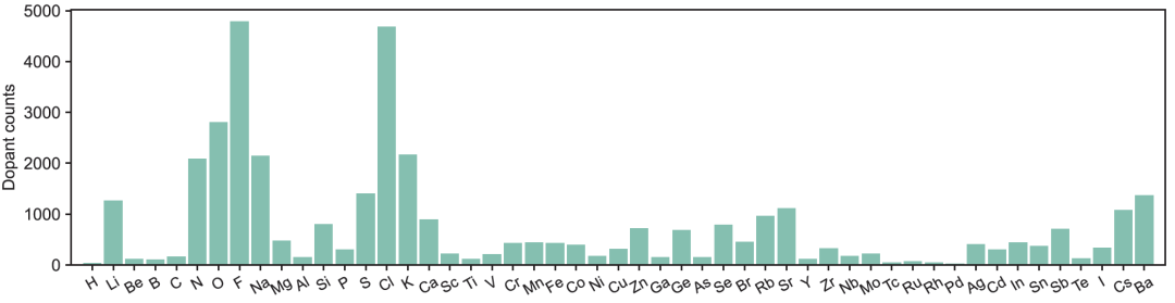
The substitution defects are selected from the first 56 elements of the periodic table (excluding the noble gas diagram), as shown in the figure below. They can be introduced individually or in combination to simulate real co-doping scenarios and provide a reference for defect engineering in future high-dimensional design spaces.
Researchers employed a machine learning recommender to guide the selection of dopants—each structure was screened for n-type and p-type dopant candidates via a dopant recommender. The parent crystal was then expanded into a supercell containing 433–500 atoms, with adaptively adjusted dimensions to ensure a lower limit of approximately 0.2% for the dilute doping concentration. Dopants were substituted into the parent lattice, and each doped structure underwent structural relaxation until all atomic forces converged below 0.01 eV/Å. After structural relaxation, the PDoS was calculated using the finite displacement method to assess vibrational properties, forming the spectral input for DefectNet.
* Structural relaxation refers to the process by which the atomic arrangement within a glassy substance gradually transforms into a more stable structure over time or during annealing.
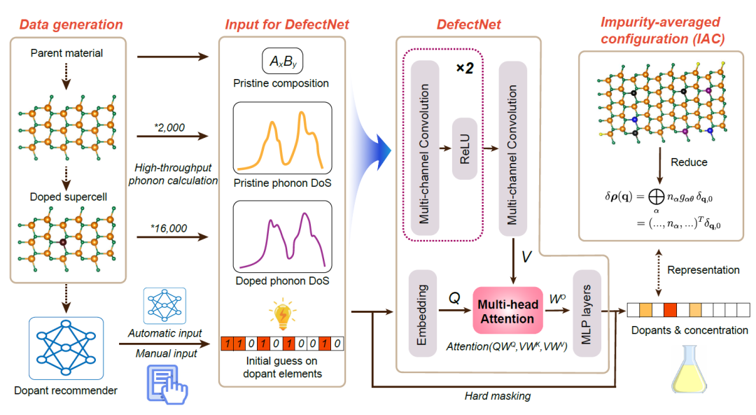
DefectNet: Non-destructively identifies the chemical types and concentrations of point defects directly from PDoS.
DefectNet is used to predict the chemical elements and concentrations of defects from phonon spectra. Its overall architecture can be broken down into 4 modules.The workflow is shown in the figure below. The goal of the model is to directly identify the chemical type and concentration of point defects from PDoS without damage.
Data Generation
After constructing the dataset, the researchers used the MACE-MP-0 basic MLIP in frozen phonon form to perform high-throughput structural relaxation and phonon calculations on perfect crystals and doped supercells. To simulate experimental resolution, the calculated PDoS curves were also Gaussian smoothed.
DefectNet Input
The model receives four types of input: the composition of the parent perfect crystal, the PDoS of the perfect crystal, the PDoS of the doped system, and an initial guess of the possible defect chemistry. The initial guess can be provided by human intuition or existing knowledge, or it can be automatically generated by a machine learning-based defect recommender, a probabilistic model used to predict the most likely dopant element. Although the training data is simulated, this framework design can be fine-tuned to adapt to experimental spectroscopic data (such as inelastic neutron scattering (INS) data).
Model architecture
The DefectNet model is implemented in PyTorch and adopts a modular architecture, consisting of four main parts:
* Spectral encoder based on 1D convolutions:The input consists of three one-dimensional signals of length 100: the PDoS of the undoped material, the PDoS of the doped material, and the host crystal composition vector. These information are concatenated into a three-channel input, and features are extracted through a one-dimensional convolutional network to finally form 100 "spectral tokens", each of which is a 128-dimensional vector.
* Dopant embedding module:The initial guesses for dopant candidates are provided as 56-dimensional binary vectors indicating the dopant elements considered for a given sample; these binary vectors are projected through a fully connected layer onto the same 128-dimensional latent space to obtain a single dopant embedding vector. This embedding vector serves as a global query for the attention mechanism, enabling the model to adjust the interpretation of its spectral features according to specific doping contexts.
* Multi-head attention mechanism:To model the interaction between doping candidates and vibrational features, DefectNet uses a multi-head self-attention mechanism, with the doping embedding as the query Q and the spectral features V as the key-value matrix. The attention mechanism follows the standard scaling dot product formula.
* Dopant-masked module:The model outputs concentration predictions for 56 doped elements, but through a "hard masking" mechanism, only candidate elements are allowed to have non-zero outputs, and the loss function is only calculated for these elements. This brings three benefits: first, it improves training stability; second, it avoids interference from irrelevant categories; and third, it maintains consistency with physical priors.
Output
The final output features are hard-masked based on the initial defect guesses, removing dopant concentrations not in the guess set. This mechanism ensures that the predicted defect concentrations of DefectNet are constrained within the initially assumed defect set; therefore, if the initial guesses are missing or incomplete, the model may be unable to recover certain dopant elements.
DefectNet can resolve 6 coexisting substitution defects.
To evaluate the capabilities of DefectNet, researchers designed a series of experiments, and the results showed:DefectNet can resolve up to six coexisting substitution defects at concentrations as low as 0.2%, and can process PDoS data without requiring detailed atomic structure information.
Application of DefectNet in Defect Type and Concentration Prediction
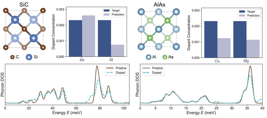
The researchers first tested typical binary (SiC, AlAs) and ternary (AgGaS₂, InCuSe₂) semiconductors on a simulated PDoS.
SiC and AlAs are highly valued in high-power electronic devices and heterostructure designs due to their large band gaps, respectively. The figure below shows the PDoS of perfect and doped crystals, as well as the predicted and actual doping concentrations. Even with low doping levels (approximately 1%), DefectNet can still capture minute vibrational changes and reliably recover the correct doping concentration.
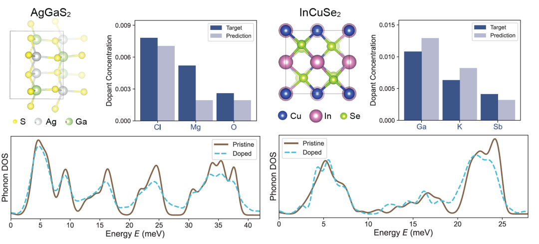
Next, the researchers applied DefectNet to the more chemically complex ternary semiconductors AgGaS₂ and InCuSe₂, with results shown in the figure below. AgGaS₂ is used for infrared nonlinear optics, while InCuSe₂ is a potential material for thin-film photovoltaics. These materials contain multiple inequivalent atomic sites and diverse vibrational modes.However, DefectNet can still track changes in PDoS and infer the doping concentration, demonstrating its robustness in complex structures and chemical systems.
To further evaluate its generalization ability, the researchers tested DefectNet on a complete defect dataset containing various coexisting dopants, including "interference" defects that are present in the input but not actually exist. The figure below shows the results by comparing the predicted defect concentrations (colored dots) with the true values (black dots), grouped by the quartiles of the mean squared error (MSE):
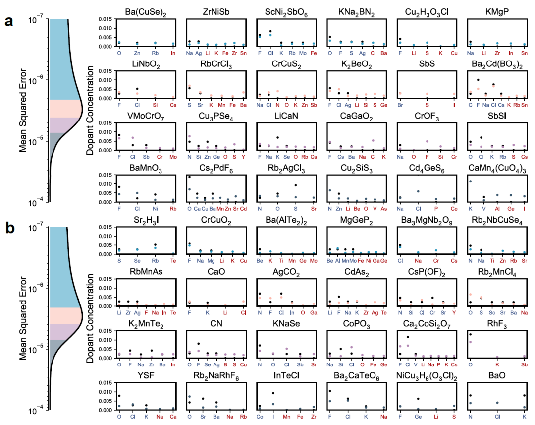
In-distribution (Figure a above): The parent crystal appeared in the training data, but its defect information is unknown;DefectNet exhibits high fidelity across a wide range of defect types and concentrations. Even when the input contains interfering defects, the model can still identify genuine doping and remove interference.
Out-of-distribution scenario (Figure b above): The parent crystal did not appear during training, resulting in a slight decrease in prediction accuracy.However, DefectNet is still able to capture the main doping features and assign near-zero concentrations to most interfering defects, demonstrating good generalization ability.
Fine-tuning DefectNet on experimental data
To verify the practical application value of DefectNet, researchers fine-tuned and tested it on experimental data. Taking thermoelectric SiGe alloy as an example, the researchers constructed a training dataset consisting of 100 amorphous Si supercells. These supercells were sampled through quenching simulations from the Si-GAP-18 database, covering various structural states from low-energy near-crystalline to highly disordered. The specific results are shown in the figure below:
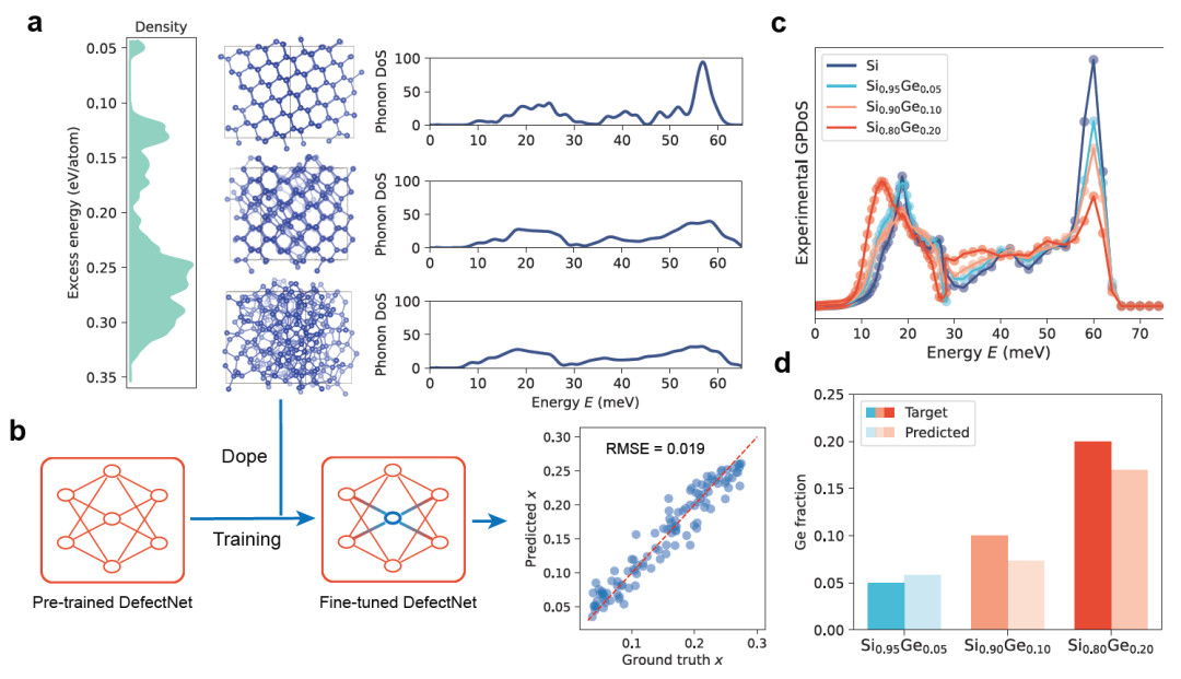
As the disorder increases, the PDoS curve broadens, and the 60 meV optical phonon characteristic peak is suppressed (Figure a above), providing a parent material for model fine-tuning. Subsequently, the researchers simulated SiGe alloys by randomly substituting Ge in amorphous Si supercells, covering various doping levels and different degrees of disorder from 0% to 25%.
After fine-tuning,DefectNet achieved a root mean square error (RMSE) of 0.019 on the test set, demonstrating strong predictive performance (Figure b above).The fine-tuned model was further applied to the experimental GPDoS data of Si₁₋ₓGeₓ alloy (x = 5%, 10%, 20%, Figure c above). DefectNet predicted the Ge concentrations to be 7%, 13%, and 22%, respectively, which were highly consistent with the experimental trend (Figure d above).
Considering the inherent difficulty of accurately quantifying defects in amorphous materials, this result demonstrates DefectNet's strong predictive ability for experimental data. For the Al-doped multiband superconductor MgB₂, the finely tuned DefectNet can reproduce experimental trends up to a doping concentration of 251TP⁻³T.
Conclusion: The prospects are broad, but the challenges are numerous.
Despite the promising prospects of this model, several challenges remain in its application. For example, at extremely low defect concentrations, vibrational features are weak and easily masked by noise, leading to decreased model sensitivity; the current version is limited to substitutional doping, and extending it to various point defect types (such as interstitials, vacancies, Frenkel pairs, or defect clusters) would significantly broaden its application scope; although the simulation data exhibits strong generalization ability, fine-tuning on experimental data remains indispensable, and achieving a model that can be directly applied to the original experimental spectra without retraining remains a long-term goal.
Looking ahead, DefectNet represents a significant step towards a unified, data-driven paradigm in defect science. Its architecture is inherently compatible with multimodal spectral inputs and opens up possibilities for inverse design of materials with specific defect characteristics. By combining physics-driven representations, high-throughput simulations, scalable learning, and experimental fine-tuning, DefectNet provides a pathway for automated, interpretable, and non-destructive defect engineering in real-world materials of full complexity.
References:
1.https://news.mit.edu/2026/mit-researchers-use-ai-uncover-atomic-defects-materials-0330
2.https://arxiv.org/abs/2506.00725